SECURE OPTICAL COMMUNICATION SYSTEM UTILIZING DEFORMABLE MEMS MIRRORS
Leah Ziph-Schatzberg[*]a,Thomas Bifanoa,b, Steven Cornelissenb, Jason Stewartb, Zvi Bleierc
aBoston University Photonics Center, 8 Saint Mary's St. Boston, MA 02215;
bBoston Micromachines Corp. 30 Spinelli Place, Cambridge, MA 02138;
cPLX Inc. 40 West Jefryn Blvd. Deer Park, NY 11729;
ABSTRACT
An optical communication system suitable for voice communication, data retrieval from remote sensors and identification had been designed, built and tested. The system design allows operation at ranges of several hundred meters. The heart of the system is a modulated MEMS mirror that is electrostatically actuated and changes between a flat reflective state and a corrugated diffractive state. A process for mass producing these mirrors at low cost was developed and implemented. The mirror was incorporated as a facet in a hollow retro-reflector, allowing temporal modulation of an interrogating beam and the return of the modulated beam to the interrogator. This modulator unit thus consists of a low power, small and light communication node with large (about 60o) angular extent. The system's range and pointing are determined by the interrogator /detector / demodulator unit (the transceiver), whereas the communicating node remains small, low power and low cost. This transceiver is comprised of a magnified optical channel to establish line of sight communication, an interrogating laser at 1550nm, an avalanche photo diode to detect the return signal and electronics to drive the laser and demodulate the returned signal and convert it to an audio signal. Voice communication in free space was demonstrated at ranges larger than 200 meters. A new retro-reflector design, incorporating more modulated mirrors had been constructed. This configuration was built and tested. Its performance and advantages as compared to the single mirror retro-reflector are discussed. An alternative system design that allows higher bandwidth data transmission is described.
1.INTRODUCTION
Retro-reflectors have been used in optical systems for some time in applications requiring a precise return of a parallel beam of light to its source. A common application uses a retro-reflector as a passive component to return incident laser pulses to the location of a pulsed laser source, allowing round trip time of flight measurement and thus precise range measurement. Active retro-reflectors are a more recent invention, and are generally retro-reflectors that can modulate an incident laser beam before returning it to the source. These so-called modulated retro-reflectors (MRRs) offer an intriguing option for laser communication, since they automatically return remote information (without the need for beam steering) to an interrogating source, and do not require transmission source at the MRR. This allows low-power, covert communication. The concept was first patented in an embodiment comprised of a retro-reflector and a liquid crystal shutter [1]. Subsequently, researchers at the Naval Research Laboratory have made considerable progress in developing MRRs using multiple quantum well (MQW) shutters [2-5]. These devices offer bandwidths of tens or hundreds of MHz, and can be quite compact. The MQW approach works over a narrow range of interrogation laser wavelengths, and is relatively expensive to manufacture. Therefore, it is not suitable for low-cost, flexible, remote-sensing applications. A number of groups have developed very short range MRRs using microelectromechanical systems (MEMS) using both MEMS corner cubes [6-8] and micro-scale cat's eye retro-reflectors [9-10]. These promise low cost, but are range limited to several tens of meters.
The present work is intended to fill a gap in these approaches: MEMS-based MRRs suitable for low-cost, compact communication over hundreds of meters. A compact, low-power device has been developed to detect and modulate an incoming laser beam, and then return the modulated signal back to the location of the sender. MRR at the heart of this device consists of a MEMS based electromechanical modulator combined with a passive retro-reflector (e.g. a hollow retro-reflector). The modulator serves as one (or more) of the three reflective facets of the retro-reflector. The MEMS modulator can be made to act as a plane mirror, maximizing the amount of light that is retro-reflected, or it can be made to act as a non-plane (corrugated) mirror, reducing the amount of light that is retro reflected. One of these states requires no power to maintain, and the other uses only microwatts. The modulation frequency can go up to at least a megahertz with conventionally processed MEMS fabrication tools and materials. Data to be sent from the MRR could include voice communication, remotely sensed environmental information, or identification information. A key attribute of this system is that the transmission power and pointing control required for long-distance communication are delivered by the interrogating beam. That is, the strength of the interrogating beam determines the strength of the returned beam (and thus the range). Furthermore, the noise-limitations for the system are contained in the receiver co-located with the sending beam. Almost no power is required at the MRR.
In this paper, design, fabrication, and testing of the MEMS modulator is detailed, and integration of the modulator with a hollow retro-reflector is described. A prototype laser communication system built with the MRR is introduced. In that prototype system, analog audio data from a microphone is frequency modulated and used to drive the MEMS optical modulator that is embedded in a wearable hollow retro-reflector. The MRR unit is interrogated by a compact laser transceiver system that is comprised of a 1.55µm wavelength 10mW laser and driver, a magnified optical visible channel and receiver, an avalanche photodiode, a frequency to voltage demodulator, and an amplifier and speaker. With this system, secure, one-way audio communication over several hundred-meter range has been demonstrated.
1.1 Principle of operation
The MEMS modulator alternates between two states: A flat state, returning most of the incident power to the source, and a corrugated state, that acts as a diffraction grating, diverting a significant amount of the light to higher orders, thus depleting the zero order return. The blinking MEMS mirror modulates an interrogating CW laser beam, returning optically encoded information to the source location, where it is decoded.
2.System description
The work described in this paper is motivated by the need to fill a gap in available MRR technology by developing and demonstrating an inexpensive MRR communication system with extended range operating at relatively low power. There is a need for systems with bandwidth greater than 100kHz, size less than 100cm3, and range up to 1 km. The basic concept of the system is illustrated in Fig. 1: An electrically modulated deformable MEMS mirror is embedded in a hollow retro-reflector, optically modulates an interrogating laser beam and returns the modulated signal to the interrogating source, where it is decoded.
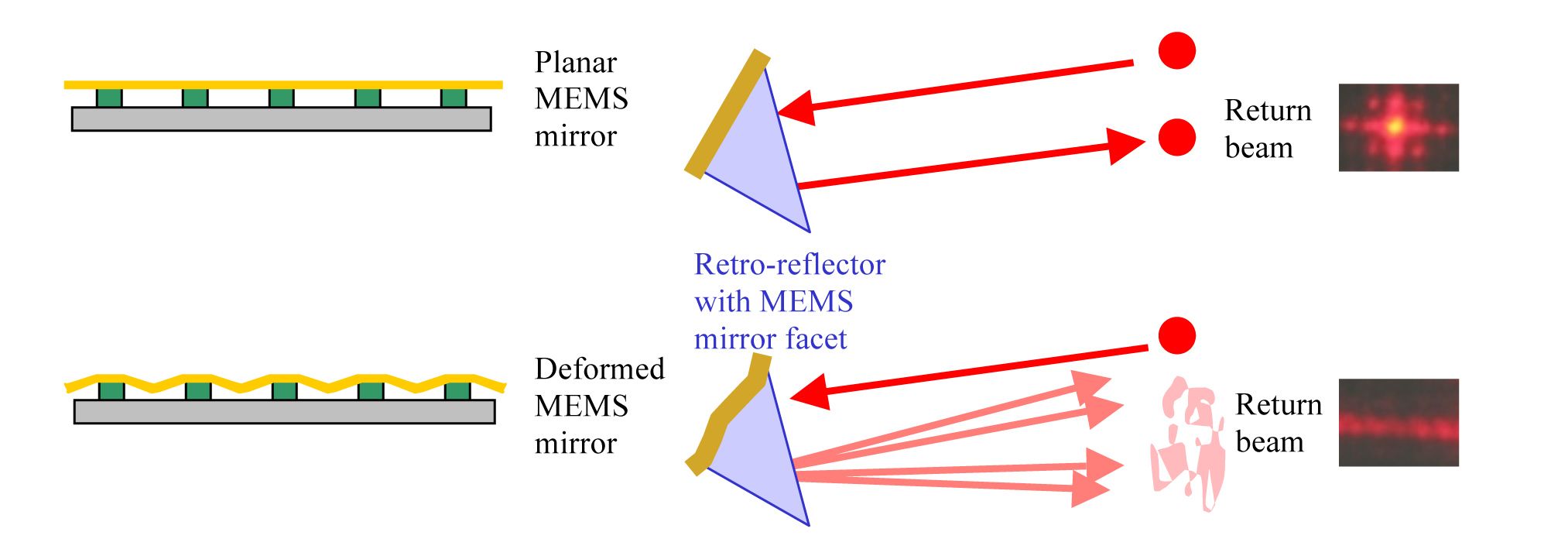
Fig.1: Principle of operation
The system is comprised of two main parts: The Retro-Communicator and Transceiver. The Retro-Communicator uses analog audio data from a microphone to frequency modulate the drive signal to the deformable MEMS mirror. The modulator is embedded in a hollow retro-reflector and thus sends the modulated signal back to the interrogator (Transceiver), where it is received, demodulated and converted back to an audio signal.
2.1 Retro-Communicator
The Retro-Communicator is conceptually comprised of two parts: The Optics Module and the Electronics Module. These two parts are combined in one small box, shown in Fig. 2.
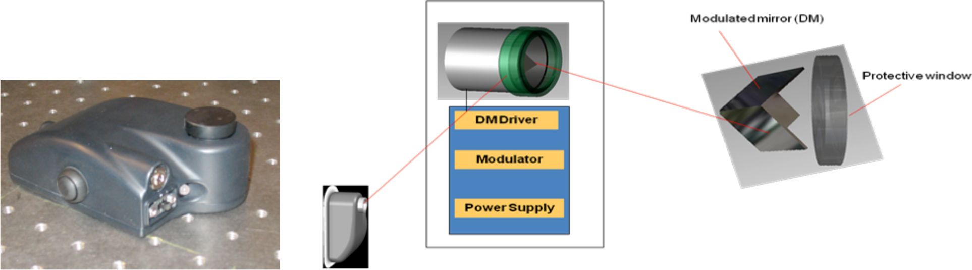
Fig.2: Retro-Communicator Module (left) and block diagram – optics and electronics (right)
The Optics Module contains the deformable mirror (DM) embedded in a hollow retro-reflector as also seen in Fig.2. The Electronics Module contains the modulating electronics to drive the DM, as well as batteries, high voltage DC power generation, and a microphone input.
2.2 Transceiver
The Interrogator/Transceiver is comprised of 1.55 mm, 10mW, CW laser, a magnified visual aiming channel and receiver, an avalanche photodiode detector, a frequency to voltage demodulator, and an amplifier and speaker. The Transceiver and its block diagram are shown in Fig. 3.
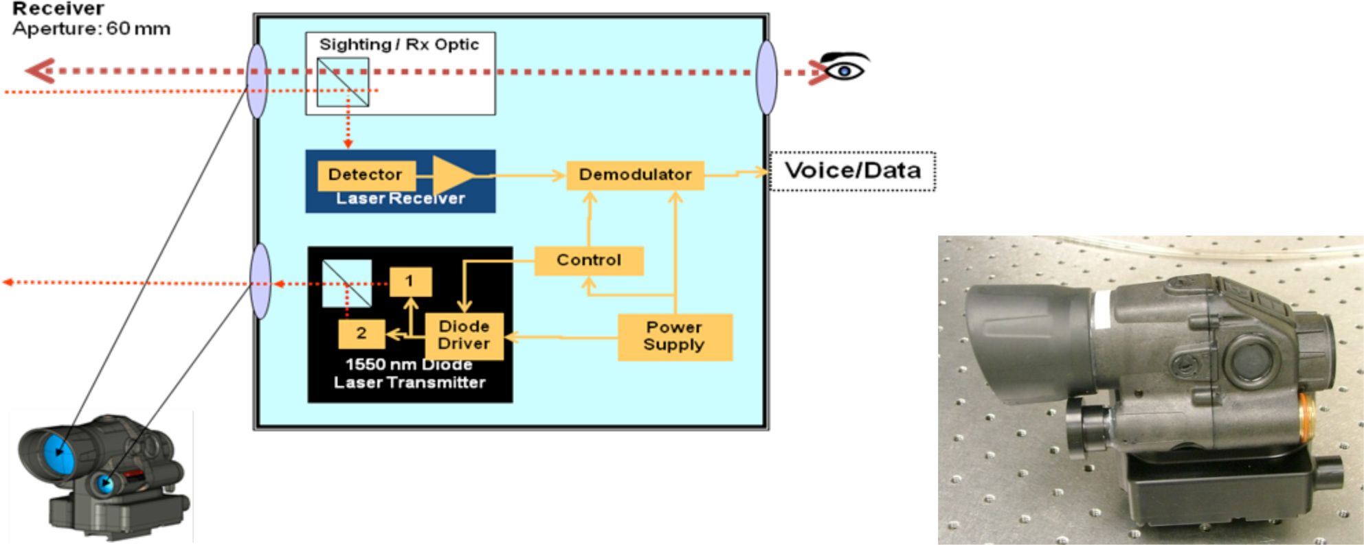
Fig.3: Transceiver and block diagram
3.Deformable Mirros
In this section, we describe the main component of the system and their characteristics.
3.1 Modulator design and fabrication
To modulate the intensity of the interrogating laser beam, a reflective MEMS mirror was designed that is optically flat in its "off" state and a diffraction grating in its "on" state, thereby deflecting most of the incident beam energy out of the reflection path. The architecture for the modulator, illustrated in Fig. 4, uses electrostatic actuation to deform rows of edge-supported narrow plates to form a diffraction grating. By maintaining the reflective gold mirror surface, supported by a tensile silicon nitride layer, at a ground potential and applying a voltage to the conductive substrate, an electrostatic force is generated between those two surfaces resulting in deflection of the flexible mirror surface.
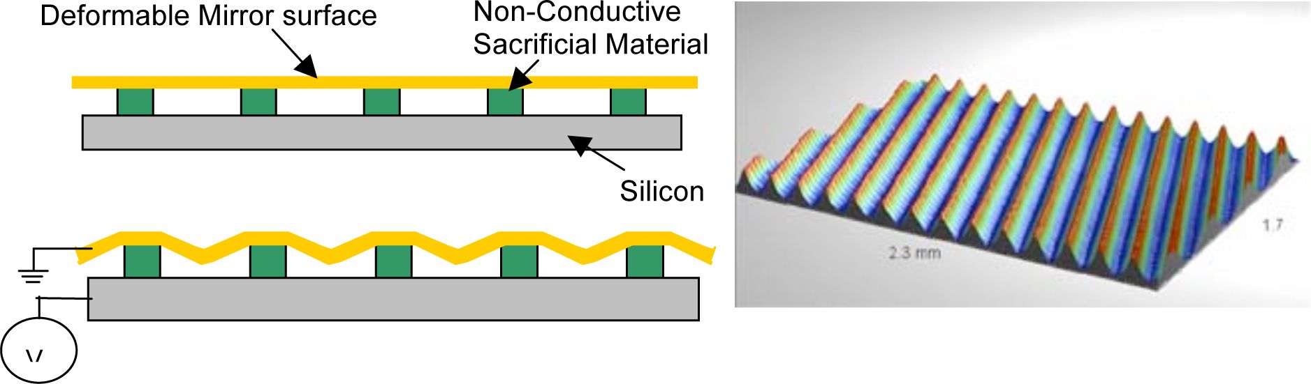
Fig. 4: Illustration of MEMS Modulator architecture
Using electrostatic actuation to modulate the interrogating beam has the benefits that the actuators consume almost no power, exhibit no hysteresis, and the deformable mirrors are relatively easy to fabricate in standard semiconductor fabrication processes. An illustration of the fabrication process flow is shown in Fig. 5.
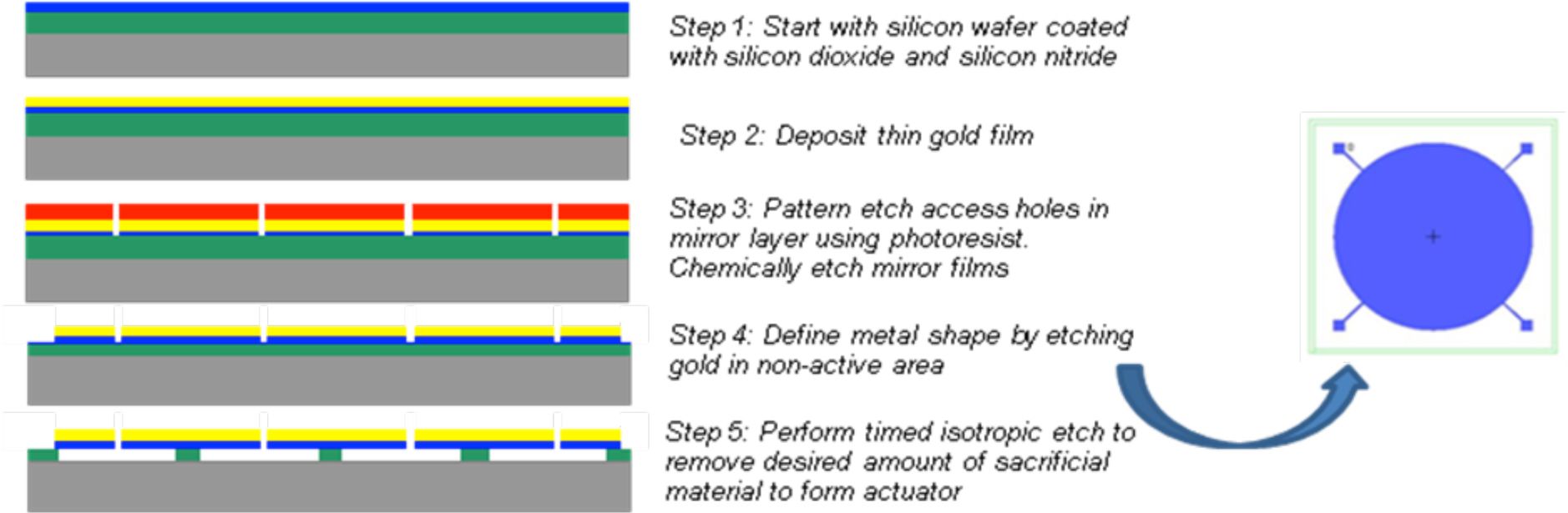
Fig.5.Schematic cross section of modulator fabrication process. The area in blue is the shape of gold film and defines the active aperture of the device.
The process uses an optically-flat, electrically-conductive silicon substrate onto which thin films of silicon dioxide and silicon nitride are deposited (step 1). A 90-nm thick gold film is then deposited using an e-beam evaporator (step 2). The gold film is lithographically patterned and etched to form small, 4-mm holes. The patterned gold film is then used as a mask to etch the small holes into the silicon nitride using reactive ion etching (step 3) that are used to define the shape of the actuators during release. The layout of the reflective gold modulator, shown in Fig. 5 (right), is defined by a second photoresist pattern which removes the gold from non-active regions (step 4). Lastly, the silicon dioxide layer is partly etched using hydrofluoric acid, leaving behind small actuator anchors (step 5) and forming the electrostatic actuators. The finished modulator has an active diameter of 9 mm.
3.2 Modulator optical and electromechanical characterizatio
Optical and electromechanical characterization of the MEMS modulators was performed using both a Wyko surface mapping interference microscope as well as an optical setup that simulated retro-reflector performance in the field. In operation, light returned from a modulator with a 9mm diameter separated at a distance on the order of a few hundred meters from the interrogating source can be described using Fraunhofer diffraction theory. When the modulator is in the "on" state, the retro-reflected beam returned to the interrogator receiver aperture corresponds to the 0th order of the diffracted wavefront. To simulate device performance in the lab, the far-field diffraction pattern is simulated using a lens located a focal length from the modulator. By placing a high speed photo detector at the Fourier plane of the lens (back focal plane), intensity changes in the 0th diffraction order can be monitored as the modulator transitions between the on and off states, providing both static and dynamic evaluation of modulator behavior.
The optical setup for the modulator characterization system can be seen in Fig. 6. The primary components consist of: A 635nm wavelength laser diode (LD) for illumination, lenses (L1 and L2) to expand the illumination beam to fill the full modulating retro-reflector mirror (MRM) aperture (at normal incidence), and lenses (L3 and L4) to project a representative far-field diffraction pattern onto a fast 2.1MHz bandwidth photo detector (PD). The photo detector uses an adjustable iris to block everything but the 0th diffraction order.
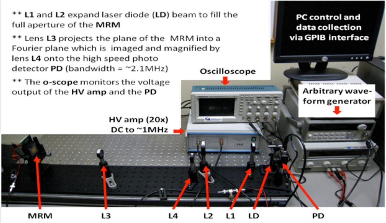
Fig.6: Modulator optical characterization system
The mirror flatness was measured using the Wyko surface interference microscope. The results are shown in Fig. 7. Typical mirror surface flatness for the full mirror aperture is about 10nm RMS. The local surface quality is also on the order of 10nm RMS, primarily a result of the etch-access holes and actuator anchor pattern.
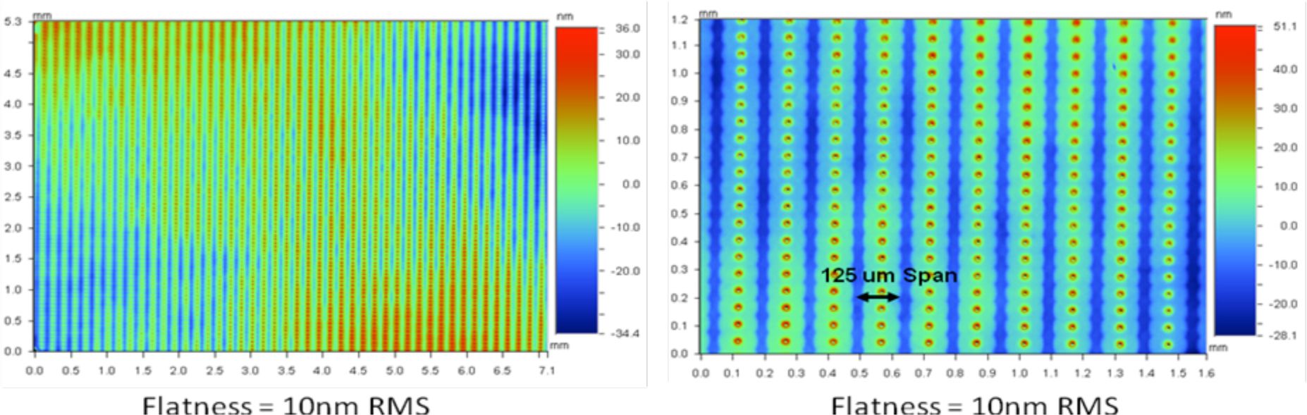
Fig.7: Surface figure measurements of the unpowered modulator: full aperture (left) and high magnification (right).
The 0th order of the "far-field" diffraction pattern is projected onto the photo detector pupil, as shown in Fig 8, such that only this order's intensity can be recorded for different modulator deflections. As previously mentioned, the detected 0th order intensity is analogous to what an interrogating illumination system would receive from the modulator in the field if it were mounted in a retro-reflector assembly. As the modulator deflects, the intensity of the 0th diffraction order decreases while off-axis higher diffraction orders increase in intensity. The output voltage of the photo detector (PDV) is recorded using an oscilloscope.
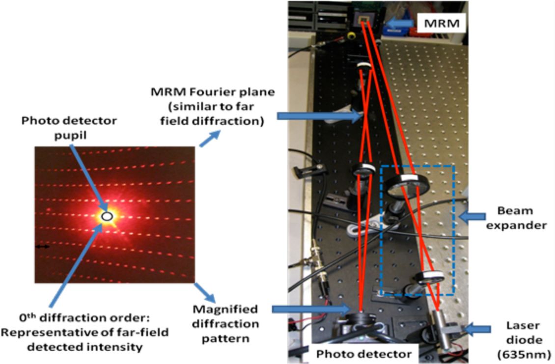
Fig.8: "Far-field" modulator diffraction pattern (left) and optical characterization system (right). Photo detector pupil located at 0th diffraction order.
Typical opto-electromechanical behavior for two modulators with a grating pitch of a 150mm, and spans of 90mm and 125mm, can be seen in Fig 9. This data was obtained using both the optical characterization system discussed above, as well as the Wyko surface mapping interference microscope. The combination of these datasets provides an empirical relationship between 0th order diffraction intensity and modulator deflection. Apparent in these characterization results is that a reduction in modulator span requires an increase in voltage to achieve identical modulator deflections. This is due to an increase in modulator membrane stiffness with a decrease in span. Stiffness is inversely proportional to span [11].
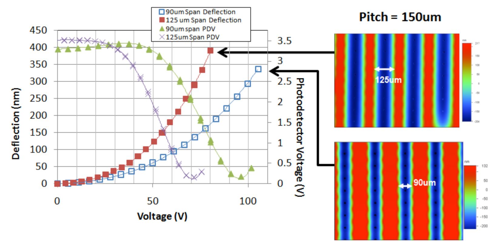
Fig. 9: DC characterization of modulators with 125mm and 90mm spans (both with grating pitch of 150mm) (Left). With increased stiffness, the applied voltage-deflection relationship for the shorter span device shifts to the right. Deflected modulator surface measurements shown at 80V and 105V for the 125mm and 90mm designs respectively.
When mounted in the hollow corner cube retro-reflector configuration, light is incident on the modulator surface at a 45 degree angle, and the plane of incidence, which is orthogonal to the plane of the grating, is rotated by 45 degrees with respect to the grating profile. This influences the phase matching conditions that create the individual diffraction orders, which reduces the modulation contrast achievable for a given modulator deflection value. In other words, the relationship between modulator deflection and 0th order diffraction intensity experiences a shift towards higher deflection, as shown in Fig 10 for the 90mm span modulator design. In order to achieve the same modulation contrast, the modulator must deflect further. Also shown in Fig 10 is that modulation contrast is uninfluenced by rotation of the grating profile with respect to the plane of incidence. At a 45 degree angle of incidence, modulation contrast remains the same when the grating orientation is rotated by 90 degrees relative to the plane of incidence.
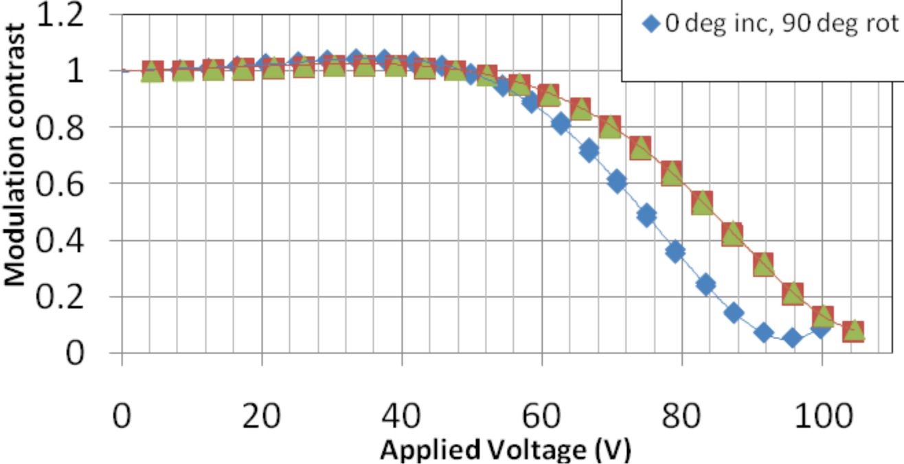
Fig.10: Modulation contrast for the 90um span device at 0 degree and 45 degree incidence. A 90 degree rotation of the modulator around its surface normal does not change modulation contrast performance. The results are scaled by the 0V contrast value.
In addition to the DC characterization of the 90mm and 125mm span modulators, the optical characterization setup was also used to perform an intensity-based measurement of modulator dynamics at standard pressure. A sinusoidal voltage was applied to these devices with variable frequency and amplitude. The modulation contrast of the detected signal at normal incidence was measured using the photo detector, and calculated as (Vmax – Vmin) / (Vmax + Vmin
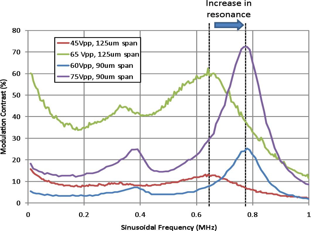
Figure 11: Modulation contrast response to sinusoidal drive voltage at variable frequencies and amplitudes.
To evaluate the influence of air damping on the dynamic performance of the modulator, the step response of the modulator to a 0 to 60V square wave (at 40kHz) was also evaluated using the optical characterization setup. The results of these measurements for the 125mm span modulator at 760 Torr and 250 Torr can be seen in Fig. 12. Here it is apparent that the prototype device behaves as an under-damped harmonic oscillator with atmospheric resonance of approximately 690kHz, and a settling time of approximately 10µs. Faster settling time could be achieved by increasing device damping through pressurized packaging, as well as changing the mechanical resonance of the MRM. Also apparent in the ringing behavior of Fig. 12 (right) is overshoot of the modulator membrane as it returns to the off-state, seen as the double peaks in the recorded data.
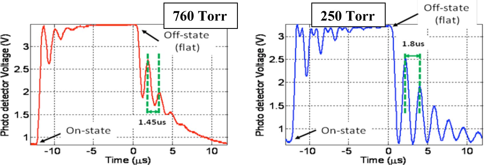
Fig.12: Dynamic response of the 125mm span modulator to a 0 to 60V, 40kHz square wave, as seen by the photo detector in the optical characterization system; 760 Torr (left) and 250 Torr (right). Atmospheric resonance was approximately 690kHz, with a 10µs settling time. The peak detector intensity corresponds to the modulator in its off (flat) state.
As previously described, the characterization of the modulator was performed using visible 635nm light, where in the retro-reflector application IR radiation with a wavelength of 1550nm is used. To understand the change in modulator performance as a function of wavelength, a model was used to determine the influence of modulator shape on diffraction efficiency. In this simulation, it was assumed that the modulator imparts a sinusoidal varying phase on the reflected beam. These results can be seen in Fig. 13 for 532nm, 635nm and 1550nm, that are the three wavelengths we used with the system, where the normalized peak intensity of the diffracted 0th order is plotted for variable modulator deflection depths. In this comparison of modulation contrast for a sinusoidal grating, similar to the modulator presented here, it can be seen that about 200nm of deflection is necessary to achieve maximum contrast in the green, about 240nm for red and about 600nm of deflection is necessary at 1550nm. The 635nm results for this model agree closely with the experimental behavior presented above in Fig. 9. Therefore to achieve optimum modulation contrast in the infrared, a larger device gap will be necessary in future devices. The present device is only capable of deflections on the order of 400nm before experiencing the unstable electrostatic "pull-in" behavior.
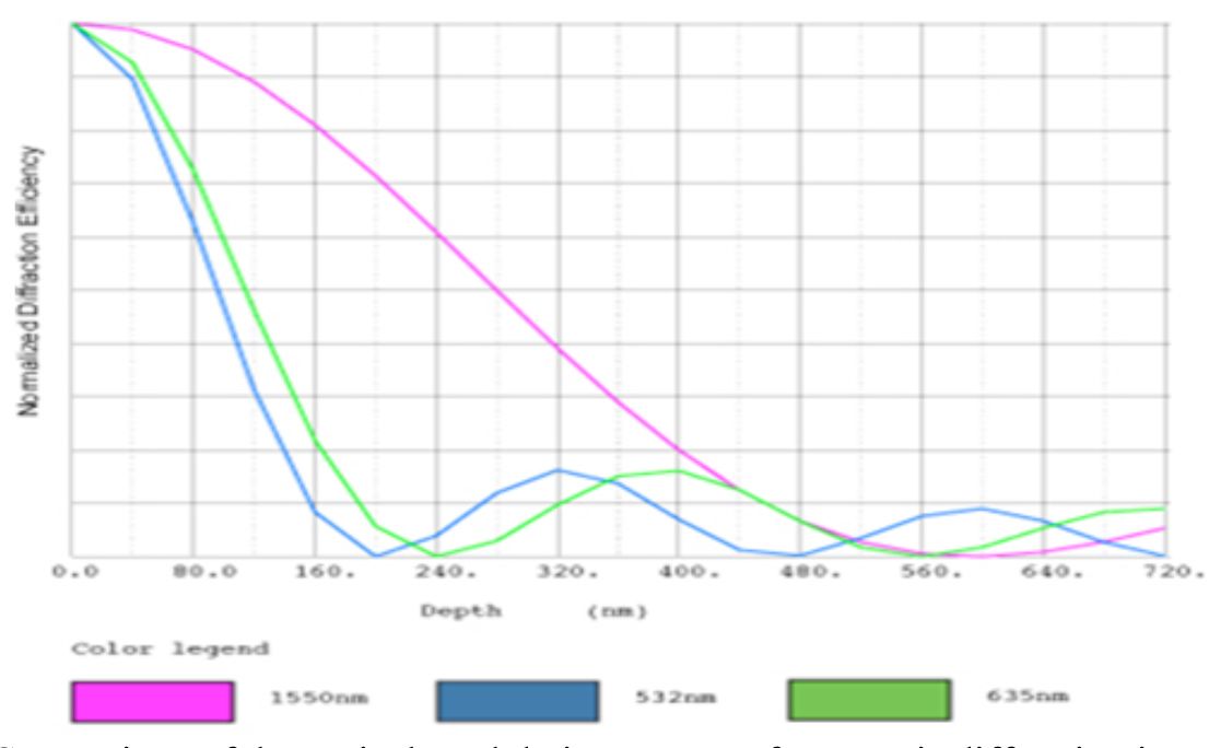
Fig. 13: Comparison of theoretical modulation contrast for on-axis diffraction intensity in visible and infrared wavelengths for a 150um pitch grating with sinusoidal cross-section. Optimum performance is achieved at a deflection of 200nm at 532nm, 240nm at 635nm and 600nm at 1550nm.
We also simulated the diffraction efficiency of the modulator at zero degrees of incidence as compared to 45 degrees. The modulator was simulated as above at 635nm; a sinusoidal grating with a pitch of 150mm. The results of the simulation are shown in fig. 14. and agree with the test results shown in Fig. 10.
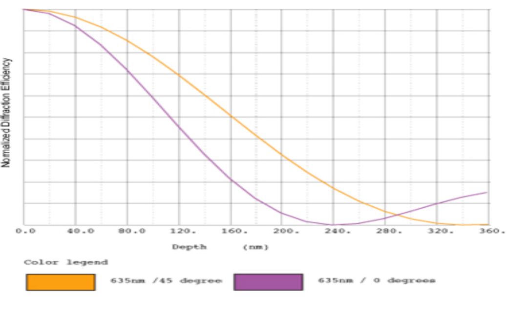
Fig. 14: Comparison of theoretical modulation contrast for diffraction intensity with on-axis and 45 degrees of incidence for a 150um pitch grating with sinusoidal cross-section. Optimum performance is achieved at a larger deflection when the illumination is at 45 degrees.
4.RETRO-REFLECTOR
4.1 Hollow retro-reflector made from silicon.
Hollow retro-reflectors are used in many applications where a parallel beam of light needs to be returned with great precision to its source. The most significant property of the hollow retro-reflector is that it works as a self compensating flat mirror that will preserve its original polarization. Silicon wafer based mirror is highly resistant to deflective distortions, having a specific stiffness (E/p - Young's Modulus divided by density) on the order of 1.5-2.5 times better than BK-7, Zerodur, Aluminum and other similar precision mirror substrate materials. The high stiffness of the silicon enables an aspect ratio of approximately 150 to achieve a six (6) waves @633nm flat polished surface, with 80 angstroms surface quality, over a 6" round wafer.
The silicon mirrors used in our retro-reflector are squares having the dimensions of 10mm x 10mm x 0.7mm. The mirrors were cut from a silicon wafer and are gold coated. Initial flatness was measured without any stress and shows 0.4 waves P.V @ 633nm. The mirror was diced from a 6" polished silicon wafer. It is evident from the flatness measured that distortion resulting from the dicing operation was kept to minimum.
Assembly of hollow retro-reflector from 3 silicon wafer mirrors presents a unique challenge. The mirrors are extremely thin, 0.7mm, they are gold coated, and the edges are not perfectly flat since they were not ground and polished. after successfully building such retro-reflectors, prototype retro-reflectors comprising of one Deformable Mirror (DM) modulator and two (2) silicon wafer mirrors were assembled. Assembly and handling the DM is even more difficult because any contact with the DM surface can deem it un-usable. Special tools were designed and built to avoid all front surface contact and handling and positioning stress. The resulting wavefront was about 0.2 waves RMS, comparable to the retro-reflector comprised of three silicon mirrors.
Subsequently, retro-reflectors assembled suing three DMs. The advantages of these retro-reflectors are the improved modulation depth as well as the ability to drive the mirrors with a 1/3 cycle delay between any two, and thus increase the bandwidth by a factor of three.
4.2 Modulated Retro-reflector performance
Measurements of the performance of the modulated retro-reflector were performed. The set-up was similar to the set-up shown in Fig.8. The only difference was incorporation of a beam splitter after the retro-reflector, and building the detection optics beyond the beam splitter. The set-up is shown in Fig. 15.
The results are, as expected, very similar to the results measured with the raw modulator, as can be seen in Fig. 16. The modulation contrast of the mirror when incorporated in the retro-reflector at a certain applied voltage is lower than the modulation contrast measured at the same voltage with the mirror when not in the retro-reflector. This can be explained when looking at Figs. 10 and 14. As can be seen in Fig. 10, the modulation contrast at 45o at the same voltage is lower than at normal incidence. Since the mirror is viewed at 45o when part of the retro-reflector, these results are consistent. The same high modulation contrast seen in the original measurements can be achieved at a higher applied voltage.
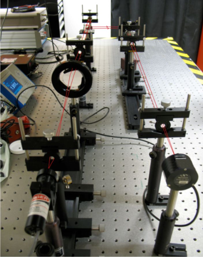
Fig.15: Modulated retro-reflector (MRR) characterization set-up
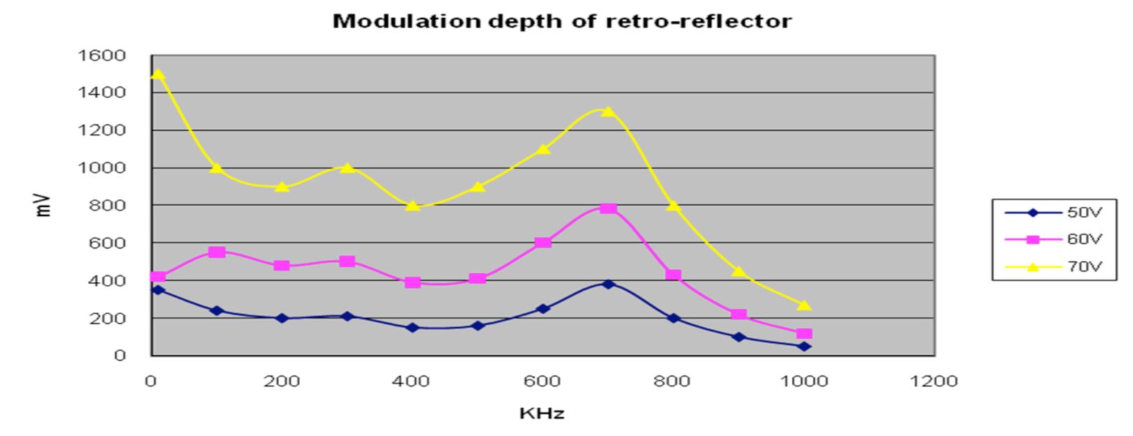
Fig.16: Modulation contrast response to square wave drive voltage at variable frequencies and amplitudes
Using a power meter we measured the modulation depth (Pmin / Pmax ) when each mirror was activated separately. Then we measured all possible combinations of two or all three mirrors activated together. Fig. 17 illustrates the measured modulation depth of all possible combinations plotted against the calculated modulation depth for the combinations. As can be seen, the modulation depth is indeed multiplicative, as we would expect.
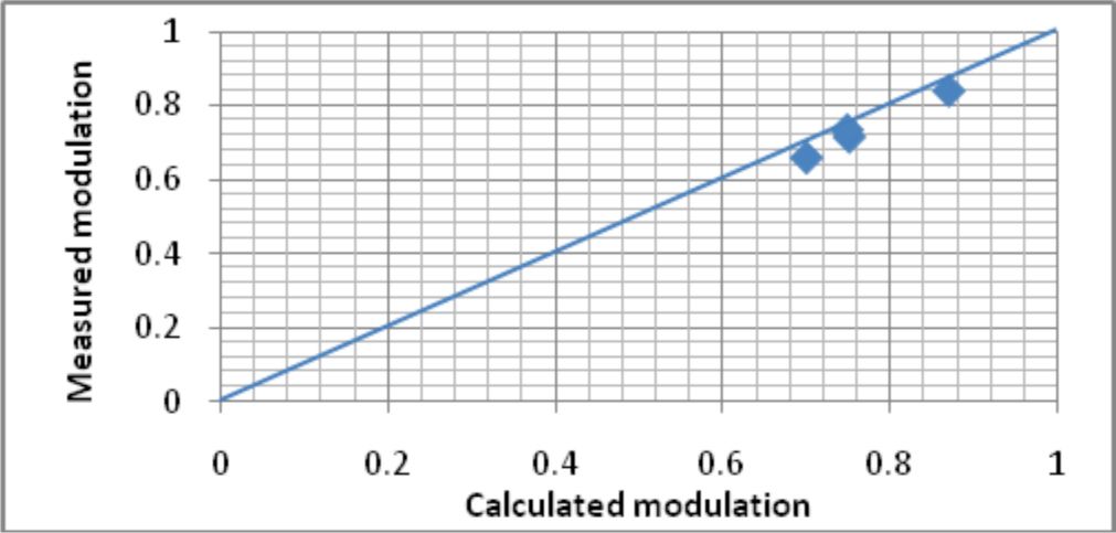
Fig.17: Measured modulation plotted against calculated modulation for all mirror combinations in a 3 DM retro-reflector
5.System Characterization
5.1 System performance
The system was tested at Devens at ranges to over 200m and performed well. The audio was clear at any range between 25 and 220m. We also performed signal to noise measurements on the system, simulating range by optical attenuation. The measurements were done with input at 1V rms, 1kHz, using a spectrum analyzer and an arbitrary waveform generator. The electronic design of the system includes an Automatic Gain Control (AGC) at the output of the demodulator. The effect of the AGC is that with a reduction in signal level, the gain increases. When the gain gets high enough for the noise to start increasing visibly, the AGC can still maintain the signal level. At the limit of the gain, the signal level starts to decline. The signal to noise measurement results are shown in Fig. 18 and meet the design goal.
The system's audio performance as a function of angle of incidence of the interrogating beam was also evaluated. The audio did not start deteriorating until about 30o off axis in each direction. Signal to noise measurements as a function of angle of incidence were performed, using the same equipment as described above. The results are shown in Fig. 18. The signal to noise measurements agree well with our qualitative audio evaluation. We saw the signal to noise deteriorate rapidly at the edge of the range/angular range. Measurements show that the audio quality deteriorates when the signal to noise ratio goes below about 25.
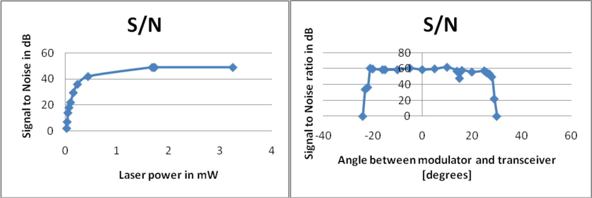
Fig.18: Measurement of signal to noise ratio of the communication system as a function of the interrogating laser power (left) and signal to noise ratio of the communication system as a function of angle between the transceiver and the modulator(right)
6.Conclusions
An optical communication system using a modulated MEMS mirror embedded in a hollow retro-reflector was constructed and evaluated. The system, using a low laser power of 10mW, demonstrated audio communication to over 200m. This system is small, low cost, low power, and could easily be extended to ranges of about 1 km. The system fills the need of a low cost, small modulated retro-reflection system with extended range. The system is particularly useful for applications when the interrogator is remote (e.g. on an aerial vehicle) and the communication needs to be covert (e.g. getting data from concealed unattended ground sensors, identification etc.).
The described measurements and analysis demonstrate that some design parameters will need to change for the next generation modulator. As seen, the mirror will need a larger range of deflection to maximize the performance at 1.55mm. Nevertheless, the system performed well with a non-ideal contrast.
Improving the deflection range of the mirror, as well as increasing the laser power, can increase the system's range to about 1 km.
7.acknowledgements
Work was supported at Boston University by Army Research Laboratory Grant # W911NF-06-2-0040, and at Boston Micromachines Corporation by Army Research Office, grant # W911NF-08-C-0006. Dr. Bifano acknowledges a financial interest in Boston Micromachines Corporation. The authors are grateful to Chad Demers for technical help in demonstrating the system, Michael Datta and Mark Horenstein for helpful suggestions regarding electronics, Michael Ciholas of Ciholas Technologies for design and development of system electronics, and Insight Technologies for help in design, integration, and testing.
8.References
[1] Fergason, James L Modulated retroreflector system United States Patent 4983021 (1991)
[2] Mark Plett, William S. Rabinovich, Rita Mahon, Mike S. Ferraro, Peter G. Goetz, Christopher I. Moore, and Wade Freeman, "Free-space optical communication link across 16 kilometers over the Chesapeake Bay to a modulated retroreflector array," Opt. Eng. vol. 47 no. 4, 045001 (2008)
[3] Peter G. Goetz, William S. Rabinovich, G. Charmine Gilbreath, Rita Mahon, Mike S. Ferraro, Lee Swingen, Robert J. Walters, Scott R. Messenger, Linda M. Wasiczko, James Murphy, N. Glenn Creamer, Harris R. Burris, Mena F. Stell, Christopher I. Moore, Steven C. Binari and D. S. Katzer, "Multiple quantum well-based modulating retroreflectors for inter- and intra-spacecraft communication" Proc. SPIE 6308, 63080A, (2006)
[4] Johan Ohgren, Fredrik Kullander, Lars Sjoqvist, Kun Wang, Qin Wang, Stephane Junique, Susanne Almqvist, and Bertrand Noharet, "A high-speed modulated retro-reflector communication link with a transmissive modulator in a cat's eye optics arrangement," Proc. SPIE 6736, 673619 (2007)
[5] W.S. Rabinovich; R. Mahon; P.G. Goetz; E. Waluschka; D.S. Katzer; S.C. Binari; G.C. Gilbreath, "A cat's eye multiple quantum-well modulating retro-reflector," Photonics Technology Letters, IEEE , vol.15, no.3, pp.461-463, (2003)
[6] Lixia Zhou, Joseph M. Kahn, and Kristofer S. J. Pister, "Corner-Cube Retroreflectors Based on Structure-Assisted Assembly for Free-Space Optical Communication," Journal of Microelectromechanical Systems, Vol. 12, No. 3, (2003)
[7] Y K Hong, R R A Syms, K S J Pister and L X Zhou, "Design, fabrication and test of self-assembled optical corner cube reflectors," J. Micromech. Microeng. 15 663-672 (2005)
[8] Trevor K. Chan and Joseph E. Ford, "Retroreflecting Optical Modulator Using an MEMS Deformable Micromirror Array" IEEE J. Lightwave Technology vol. 24 no. 1 pp. 516-525 (2006)
[9] C Jenkins, G Brown, W Johnstone and D Uttamchandani, "Microelectromechanical systems actuated small-scale retroreflectors for free space optical communications," J. Opt. A: Pure Appl. Opt. 8 S384–S390 (2006)
[10] Jenkins, C., Johnstone, W., Uttamchandani, D., Handerek, V., and Radcliffe, S., "MEMS actuated spherical retroreflector for free-space optical communications," Electronics Letters , vol.41, no.23, pp. 1278-1279, (2005)
[11] Stephen Senturia, "Microsystem design", Kluwer Academic Publishers, Boston, 2001.
[*]lzs@bu.edu, Tel: 617-353 8907, www.bu.edu/photonics